|
[CVD I]
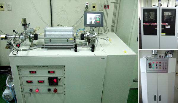
- IV (Si,Ge) semiconductors
- Gas cabinets (top right) with gas-leak detector & automatic valve shutters
- Gas scrubber (Bottom right)
|
[MOCVD system]
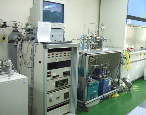
- II-VI oxide semiconductors
- ZnO nanorods and nanomaterials
|
|
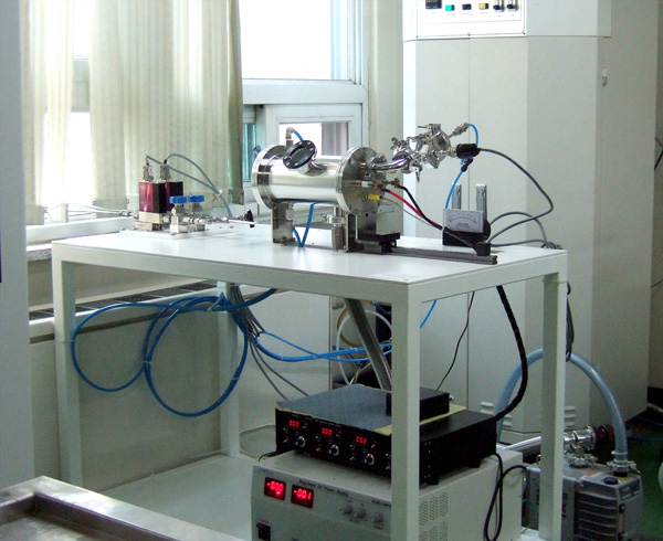
[CVD II]
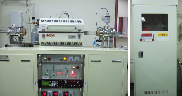
- III-V semiconductors
- Gas cabinets (right)
|
[Evaporator]
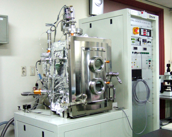
- metal deposition
|
|
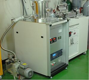
[CVD III]
- Carbon based materials synthesis
|
[RTA]

- Thermal annealing
|
|
[Plasma etcher]
- Oxygen plasma etcher
|
[Optical microscopy]
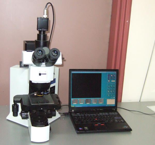
- Olympus BX51
|
|
[Electrical measurement system I]
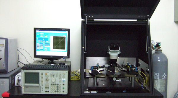
- Probe station
- Semiconductor parameter analyzer
|
[Electrical measurement system II]
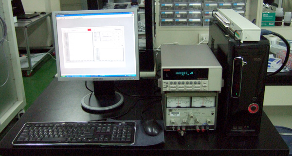
- DAQ
- Picoammeter
- Voltage amp./bipolar power supply
|
|
[Electron beam lithography system]
- NPGS
- SEM (MSE facility)
|
[Optical measurement system]
|